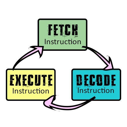
What is the Fetch Decode and Execute cycle of a computer system?
Watch this or read the blog post below for a detailed explanation of how the Fetch Decode Execute Cycle really works!

The basic operation of the Central Processor Unit utilises what is called the ‘fetch-decode-execute’ cycle. The CPU is designed to load, read and execute a set of instructions – the CPU instruction set. It fetches the instructions from the main memory, decodes them, and executes them. This is done repeatedly from when the computer is booted up to when it is shut down, and is done at amazingly fast speed!
- The CPU fetches the instructions one at a time from the main memory into the registers. One register is the program counter (pc). The pc holds the memory address of the next instruction to be fetched from main memory.
- The CPU decodes the instruction, splitting it into operator and operand – Ill explain that later below!
- The CPU executes the instruction.
- Repeat until there are no more instructions.
A single piece of program code might require several instructions. For example here is some python code :
area = length * width
First, the computer needs to load in the value of the variable length into the memory registers. Next it needs to load in the value of the variable width into the same registers, but in a different location within the register. Then it needs to multiply the two numbers together. Having done this, it finally needs to store the result in the variable area.
Instruction address Program counter to Memory Address Register
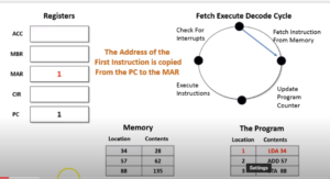
In the diagram above, you will see a number of registers, two areas of memory, and the stages of the Fetch-Decode-Execute cycle. Let me explain them :
ACC – This is the Accumulator, and is the register where intermediate arithmetic and logic results are stored. This saves the data being written and read twice into main memory. Main memory tends to be slower than the accumulator or any other register, and it is cheaper.
MBR – A memory buffer register (MBR) (also known as memory data register (MDR)) is the register in a computer’s processor, or central processing unit, that stores the data being transferred to and from the immediate access storage. It contains the copy of designated memory locations specified by the memory address register.
MAR – memory address register (MAR) – holds the address of the current instruction that is to be fetched from memory, or the address in memory to which data is to be transferred.
CIR – Current Instruction Register – In computing, the instruction register (IR) or current instruction register (CIR) is the part of a CPU’s control unit that holds the instruction currently being executed or decoded.
PC – Program Counter – The program counter (PC), commonly called the instruction pointer (IP) is a processor register that indicates where a computer is in its program sequence.
Memory – This consists of the address of the the memory location, and the contents of that location. The Trick is to use the memory address to find the data of that location, and then move that data (whatever it is) into the required register for it to be operated on (The Operand).
In the first diagram above, the program counter is read into the MAR.
Executing the first Instruction…..
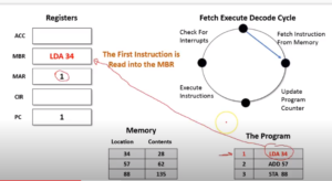
In the diagram above, With the MAR contain “1”, the processor will then fetch the contents of that address, which is the first line of our program. This 1st instruction is read into the MBR – Memory buffer Register. The Memory Address Register and program counter contain the address of the 1st instruction.
The Diagram below shows the Instruction in the MBR now being loaded to the CIR (Current Instruction Register. This is the fetch phase of the cycle
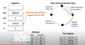
The program counter is now incremented and will point to the next instruction in the program memory.
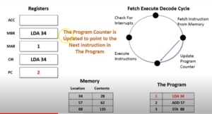
In the diagram below, the address part of the current instruction is placed in the MAR. It indicates the location of the next piece of data to be loaded. This is the decoding phase of the cycle.
Operand and Operator. The Instruction LDA 34 consists of an operator and a operand. In this case LDA is the operator, and 34 is the operand. In all computer languages, expressions consist of two types of components: operands and operators. Operands are the objects that are manipulated ( in this case “34”, and operators are the symbols that represent specific actions (LDA performs a specific action).
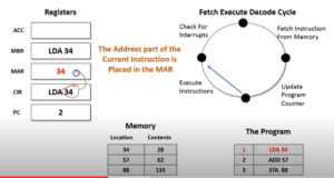
In this diagram, The contents of this MAR register will be loaded into the MBR Register for some operation to occur on that data.
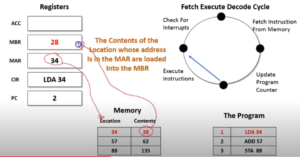
In this diagram, the contents of the MBR are now loaded into the ACC. At this point we can see that the instruction has now been executed.
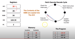
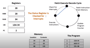
In this diagram it shows that the status register is checked to see if there have been any interrupts. But What is an interrupt?
In digital computers, an interrupt is a response by the processor to an event that needs attention from the software. An interrupt condition alerts the processor and serves as a request for the processor to interrupt the currently executing code when permitted, so that the event can be processed in a timely manner. If the request is accepted, the processor responds by suspending its current activities, saving its state, and executing a function called an interrupt handler (or an interrupt service routine, ISR) to deal with the event. – https://en.wikipedia.org/wiki/Interrupt
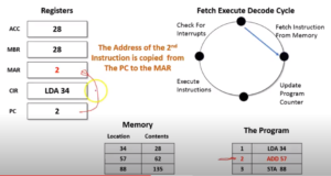
The program counter contents are copied to the Memory Address Register. so to retrieve the data to be found in that location.
The 2nd instruction is read into the MBR. This 2nd instruction is contained in the contents of the program address “2”
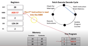
The contents of the MBR are now moved to the Current Instruction Register

The program counter is now updated to point to the next instruction in the program memory

The Address part of the Current Instruction Register (The Operand) is placed into the MAR
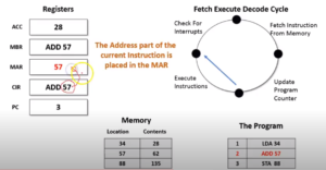
The Address which is in the MAR, the contents of this register are then loaded into the MBR.
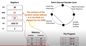
The contents of the MBR are then added to the ACC. This will give us an accumulator value of 90 – remember that the previous value was 28, and adding 62 we get 90!

Following a successful instruction completion, the Status register is checked for Interrupts
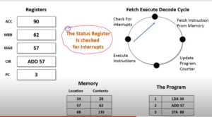
A new instruction is now ready to be fetched, decoded, and executed. the Address of the program counter now goes to the MAR.
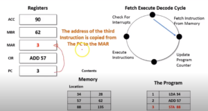
The third instruction is read/loaded into the Memory Buffer register
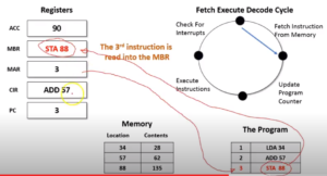
The third instruction is copied into the CIR.
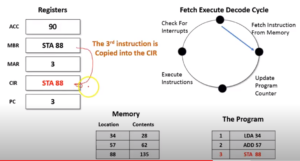
The program counter is now incremented for the next instruction to come along from the program memory.
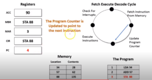
The address part of the CIR (the operand) is placed into the MAR – Memory Address Register
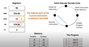
We have a STA 88, which means that the contents of the ACC will be stored in memory location 88. So in this diagram, the contents of the ACC are moved to the MBR.

Here the contents of the MBR are now copied into the memory location 88.
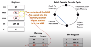
This diagram shows how the contents of the MBR are now copied into the location 88, and the contents change from 135 to 90.
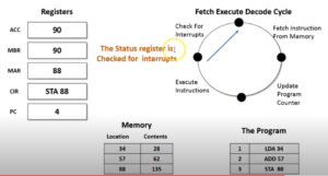
The status register will now check for interrupts as the Fetch Decode Execute cycle is now complete, for this instruction, and our program.

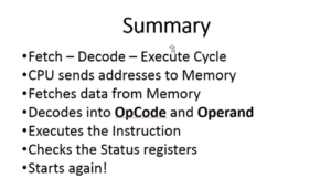
Finally, here’s the summary for the fetch decode and execute cycle :
I do hope this has been helpful in your understanding how this process works. You’ll probably have to go through the article or the video a number of times to ensure that you really have grasped the concepts. Once you have, they will really help your understanding of what computers can do!
References :
